CHIPnGo Dev #12 - The PCB
With power requirements sorted and all components selected, I spent the next few days voraciously consuming as much as I could regarding PCB design. I decided to use KiCad as my design tool of choice, since it was free and there appeared to be a lot of resources available for learning it. Once I had a general understanding of how to use it, it was time to get started.
I had learned that there were three main steps of PCB design:
- Creating the schematic
- Creating/placing footprints (layout)
- Routing traces
Schematic
So I started with designing the component symbols for use in the schematic. Luckily there was already a bluepill symbol available so that just left the display and SD breakout. Designing the symbols was pretty straight-forward, and all I had to do then was connect them according to how I had everything wired on the breadboard. I tried to follow some of the best practices I had read about and make it as clear as possible, and after performing an electrical rules check, everything seemed to check out. Below you can see the final schematic, though there was a slight variation before this (which I talk about briefly in the layout section).
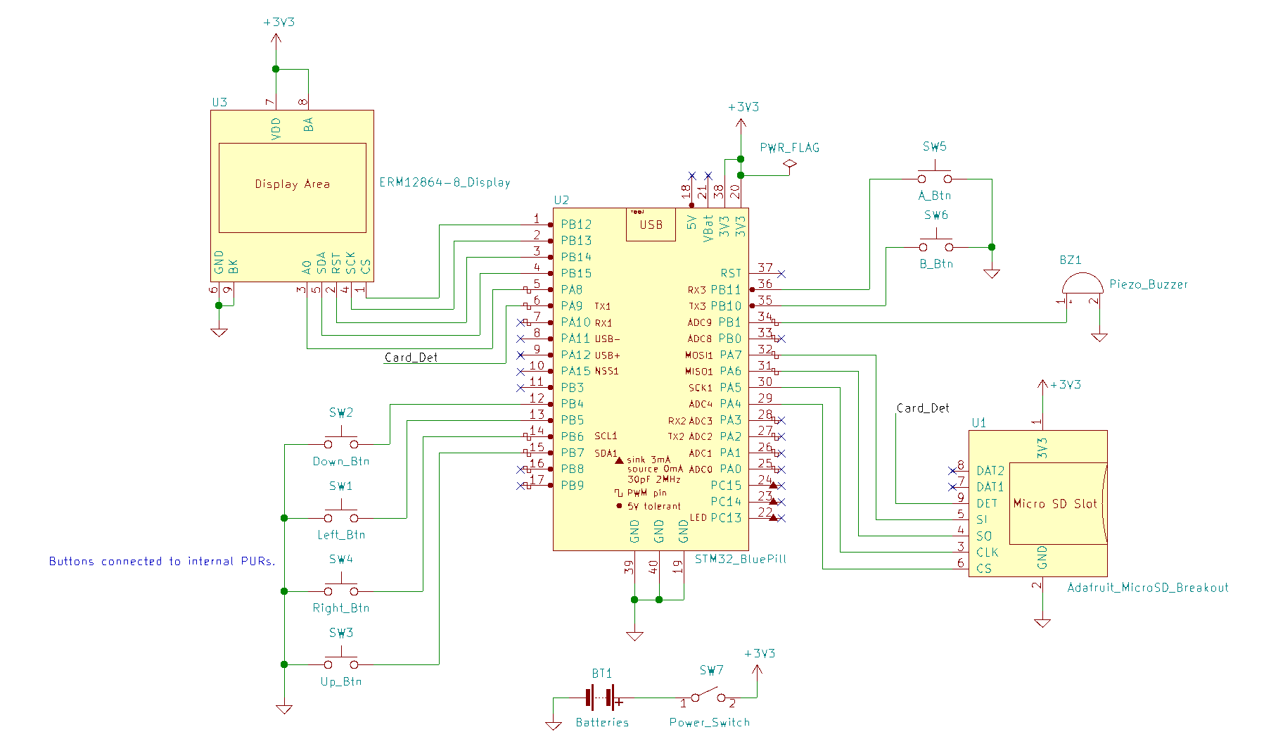 With the breakout boards already including resistors, capacitors, etc, all I had to do was draw connections between pins.
Layout
Most of the components, including the bluepill, already have footprints available, so that saved me a lot of time. However, I’d still have to manually design the footprints for the display and SD reader and this was a bit tricky. I had to ensure that all the measurements were precisely correct, including the size and spacing of the drill-holes/copper pads for the pins.
Luckily the datasheets were helpful in providing the measurements, however the datasheet for the display seemed to have things flipped. Fortunately I had the physical display on me during this time to verify this, so that potentially saved me a major headache. I decided not to make use of the mounting holes for the display and SD reader as I didn’t feel they were really necessary, but if I was trying to make this more rugged I would likely include them for extra stability.
Once the footprints were all complete, next I had to begin laying them out. As mentioned previously, I was going for a GameBoy Advance style where the display would be in the center with the buttons on either side. Typically, it seems with PCB design you want to try to lay components out in a way that makes routing easy and uses up minimal space. But, I had to take ergonomics into account since this PCB was meant to actually be held which meant making the PCB larger (thus driving up production cost) and placing components in a way that might make trace routing trickier.
Ultimately, I settled on this layout, where the bluepill and battery holder would be placed on the backside, and the display and SD reader centered on the front side. The final size was 165mm x 78mm (6.5in x 3in) which is a little bit larger than my iPhone X.
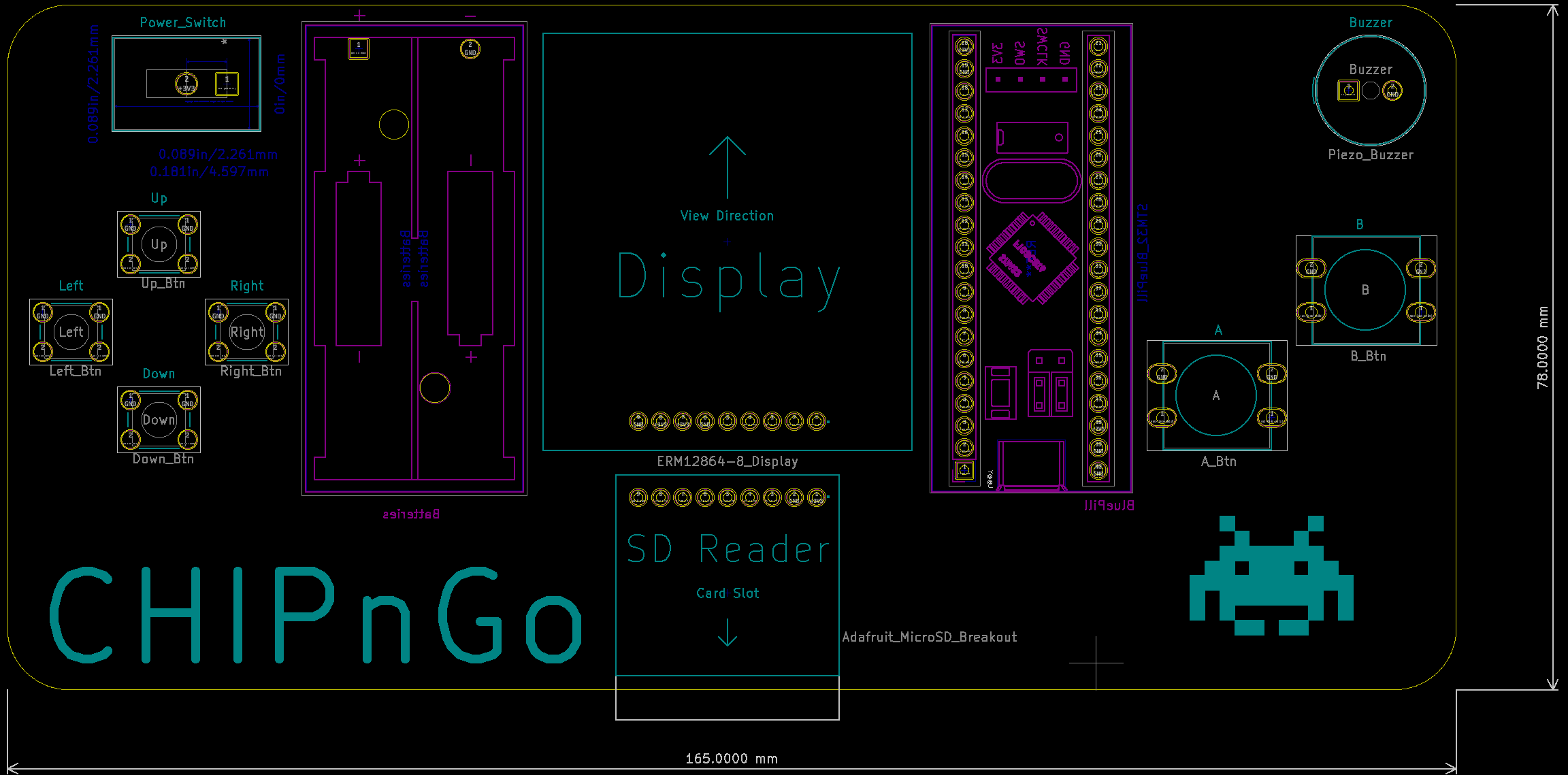 A lot of unused space, but I had to consider ergonomics.
Routing
This was the part I was most worried about, since it seemed there was a lot to take into account when it comes to routing. Things like trace width and spacing, proper use of vias, etc seemed quite overwhelming and if I didn’t get things right there was potential for the entire PCB to fail. However, I was hoping that since I wasn’t making use of any analog or high-speed signals, and that I was working with relatively low current, that I would be able to get away with quite a bit.
I had decided on going with OSH Park as my manufacturer so before I began I entered their design rules. After that, I decided on signal traces of 0.25mm and power traces of 0.5mm. My first attempt ended up looking quite ugly and and I was using multiple vias and running traces on both sides just to get everything to connect.
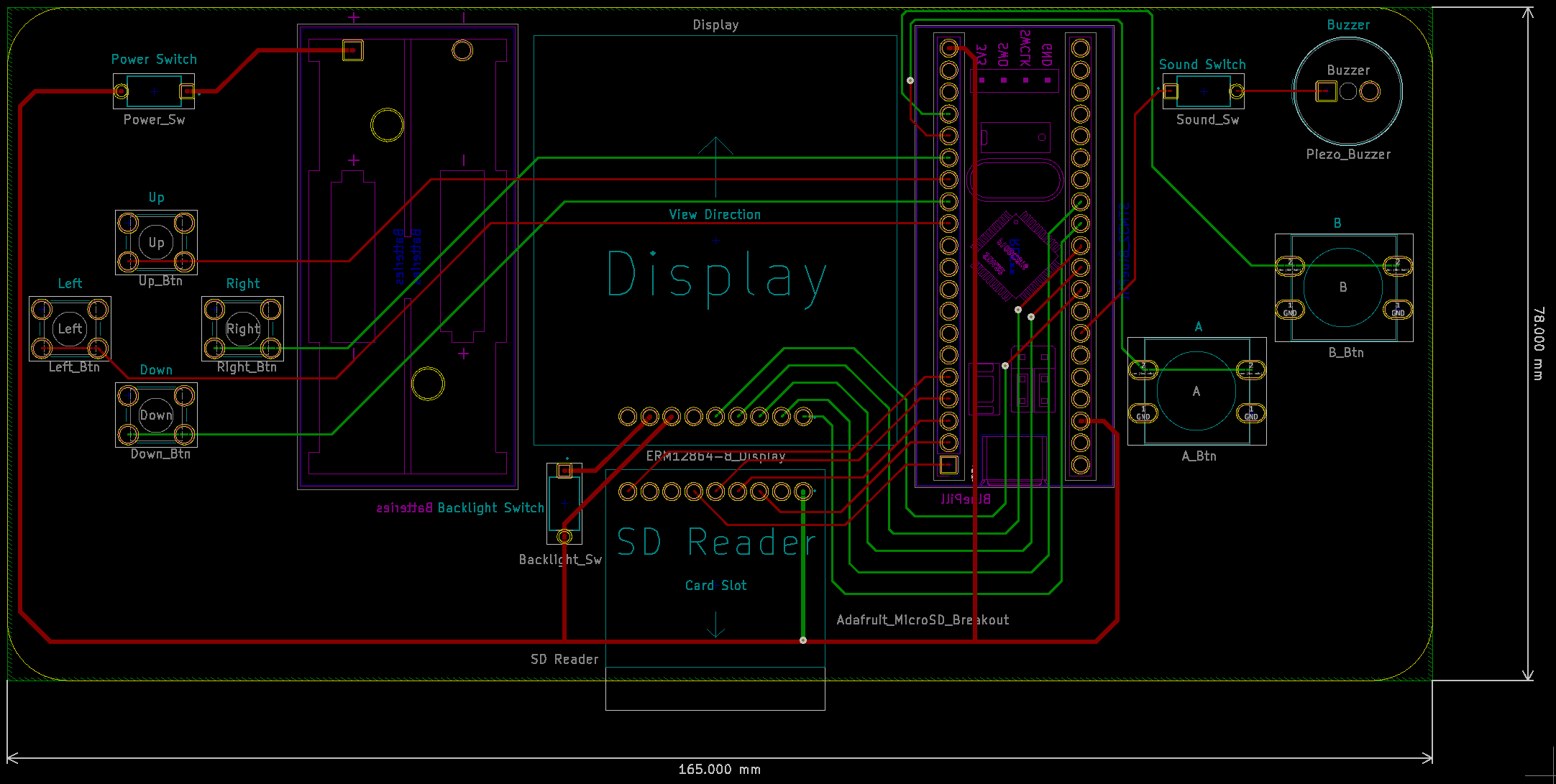 This just won't do (ignore the extra backlight/buzzer switches which weren't in the final product).
Not satisfied, I decided to rewrite some of the firmware to use different pins to make routing cleaner. After testing this on the breadboard, and updating the schematic to reflect these changes, I went back and rerouted the traces to be a bit less ugly. I also had read that it can be a good idea to increase trace widths if you have the extra space, so I increased signal traces to 0.5mm and power traces to 1mm to be on the safe side. With this, I was able to keep all signal traces on the front side and just stuck the power traces on the backside.
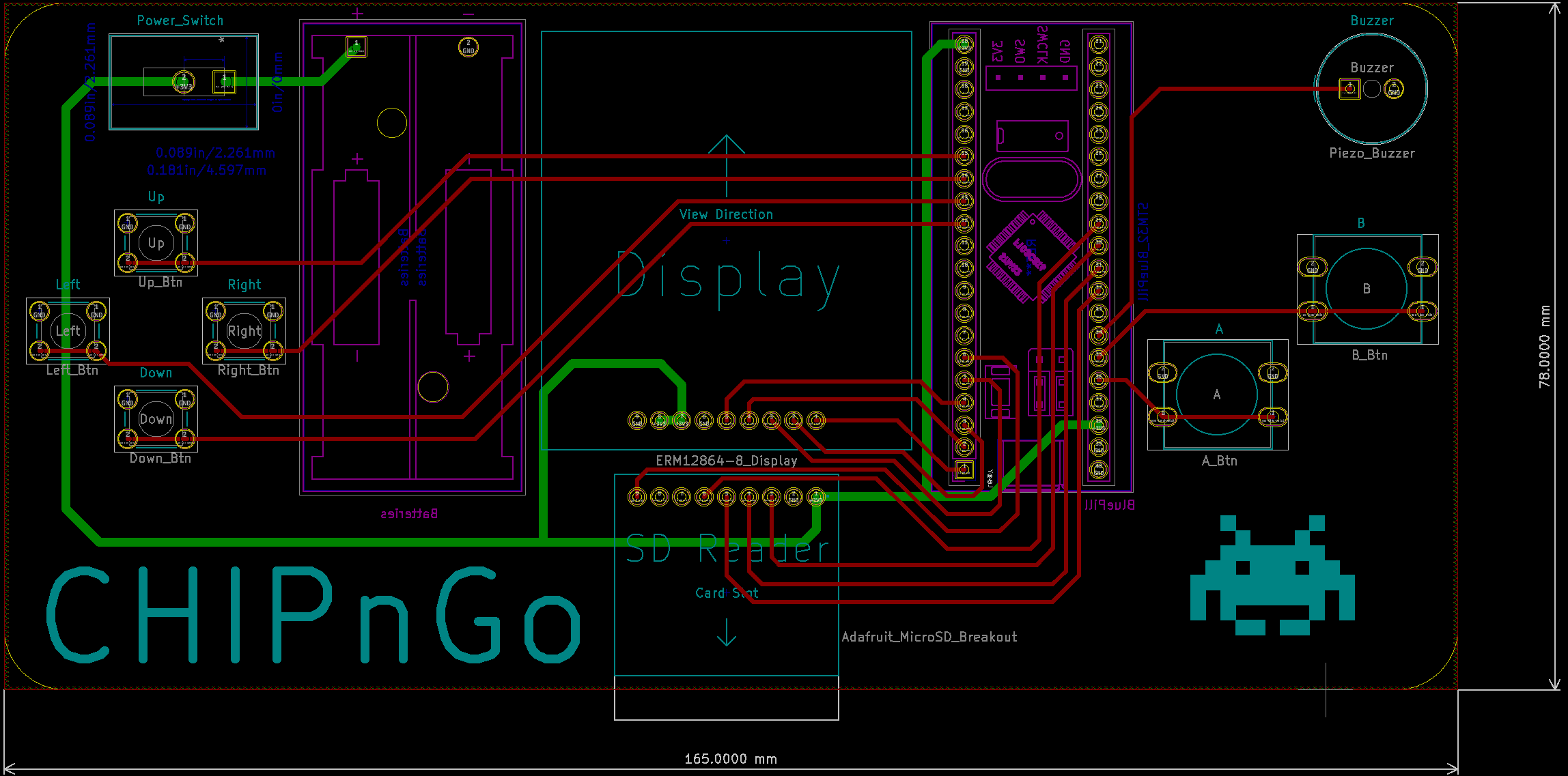 Things are looking a bit cleaner.
Really all that was left was deciding how to handle ground. Based on my reading it seemed that the best way was to make an entire ground plane and just connect the ground pins to this plane. Some also suggested having a ground plane on both sides and use vias to connect them, but I didn’t fully understand why/where to place the vias, so I just settled on ground planes on both sides, but with no vias, and hoped for the best.
After triple-checking my schematic and footprint measurements (I printed a 1:1 scale paper copy and made sure the components lined up properly), I took the plunge and ordered my PCBs. Due to their size, it would cost me roughly $90 for a set of three from OSH Park. Oof. I still wasn’t entirely sure this thing would work, so I was worried I had made an expensive mistake, but there was only one way to find out.
| << Prev | Next >> |